Materials, microelectronics, acoustics, nanotechnologies (GREMAN)
20, avenue Monge - Bât.E
Tours 37200
France
GREMAN specializes in materials, components and systems for electrical energy management and conversion with the aim to improve energy efficiency. Thanks to the knowledge of its four teams, which deal both with materials sciences (solid-state physics and chemistry) and engineering sciences (microelectronics, ultrasounds, electrical engineering), it can carry out work from the synthesis of new materials with remarkable properties to the development of components and devices and their integration in electrical systems.
Applications range from new microelectronics components, both active and passive, transducers and ultrasound systems, systems for electrical energy conversion.
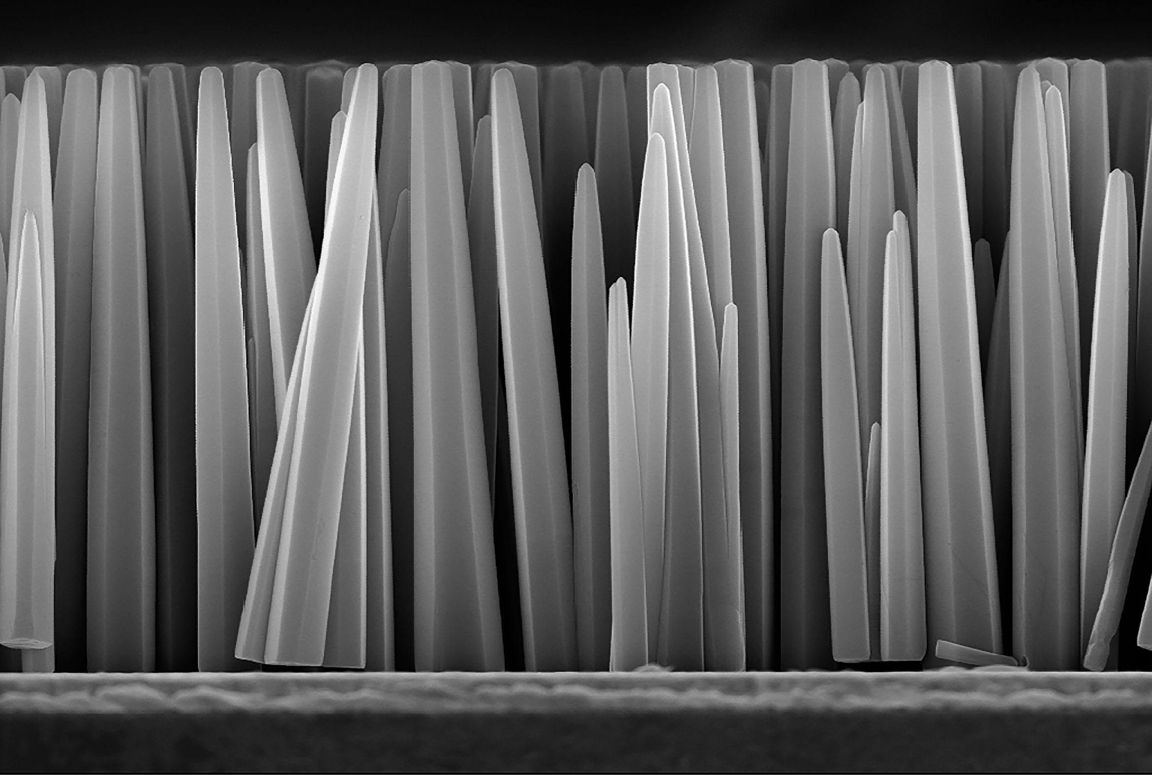
Its research activities include fundamental studies involving simulation tools and models developed within the laboratory. They benefit from a range of technological platforms including the CERTeM (Centre d’Etudes et Recherches Technologiques en Microélectronique) for multiphysics and multiscale fabrication and characterization.
Research topics:
- Oxides for energy
- Magnetic and optical properties of multiferroic and electronic correlated materials
- Ultrasonic devices and characterisations
- Energy, Components, systems, microelectronics
Experimental tools:
- 2400 m² clean rooms (ISO 5, 7 and 8), lithography, plasma etchings (RIE, IBE), annealing (RTA, high temperature, laser)
- Deposition methods (PVD, PLD, LPCVD, PECVD, ALD, spin coating)
- Synthesis of powders and ceramics (Spark Plasma Sintering), single crystals (image furnace)
- Structural, micro-structural and chemical characteri- zations (MEB, MET-STEM-EELS, FIB-STEM, diffrac- tion X, WDS, EDS, AFM)
- Electrical measurements: DC and RF under probes, anechoic chamber, PPMS, AFM
- Optical measurements: spectroscopy (IR, visible, UV, Raman), ellipsometry, laser interferometry and vibro- metry, holography, Kerr magnetometer, SNOM
- Thermal measurements: laser flash, thermoelectric (ZEM-3, PPMS), SThM, thermoreflectance, PPMS
 |
|
|
CURRENT AND PAST FELLOWS IN RESIDENCE


Events


